

Decoding the Physical Essence Behind Memory Compiler Parameter Configuration
2026-09-10
—— From Mux, Bank to Vt, Deeply Disassembling the PPA Trade-off Nature of SRAM
IPSoar Technical Popularization
Abstract: In SoC chip design, the PPA performance of SRAM profoundly affects the competitiveness of chip projects. The Memory Compiler (MC) comes with a large number of adjustable parameters, which support fine-grained parameter tuning for SRAM instances. Simply knowing how to adjust parameters is far from enough. Understanding the physical principles behind the parameters is an important basis for helping designers make reasonable PPA trade-offs. Continuing with our previous MC IP technical popularization content, this paper analyzes the influence logic of key parameters Mux, Bank and Vt on SRAM area, performance and power consumption from the physical essence, to assist engineers in memory IP selection and reduce back-end iteration.
1. Column-Mux: Reshaping the Memory Array Form to Realize the Basic Trade-off Between Area, Speed and Power Consumption
The Mux in the Memory Compiler usually specifically refers to Column-Mux. Under the premise that the Word count and Bit width of an SRAM are fixed, the Mux configuration directly determines whether the physical layout of the memory array is "tall and thin" or "short and stout", which is the root cause of its impact on PPA.
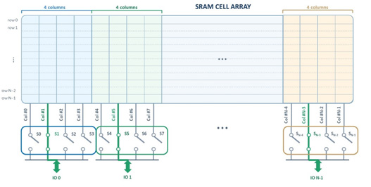
Taking a memory instance with Word=128 and Bit=8 as an example, when Mux is set to 2, 4 and 8 respectively, the physical shape, row count and column count of the memory array will change significantly, as shown in the table below:
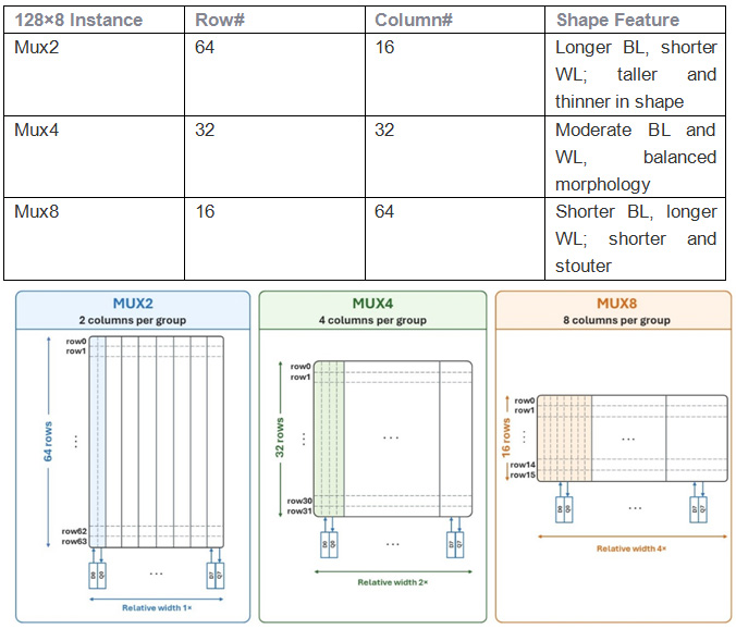
The essence of the above changes can be precisely defined by the following formula — when Word and Bit are given, the number of Rows and Columns is completely determined by Mux:
Row = Words / Mux
Column = Bits × Mux
It can be seen that the direct effect of increasing Mux is to reduce the number of rows and increase the number of columns. Reflected in the physical layout, this means shorter Bit Lines (BL) and longer Word Lines (WL), making the entire array evolve from "tall and thin" to "short and stout". It is this change in shape that triggers a series of chain reactions in area, speed and power consumption.
In-depth Analysis of Physical Mechanism
•Bit Line (BL) Load Effect: The bit line is a metal trace running through an entire column, with a large number of memory cells connected in parallel on it. The longer the BL, the larger the parasitic capacitance, the longer the charge and discharge time, which directly slows down the read and write speed and increases dynamic power consumption. Therefore, shortening the BL is an important means to improve performance.
•Word Line (WL) Load Effect: The word line extends along the row direction. The longer the WL, the greater its Resistance-Capacitance (RC) delay, and the longer it takes to select an entire row. Therefore, an excessively long WL will also become a speed bottleneck.
•Trade-off Essence: The adjustment of Mux is essentially a trade-off between "long BL + short WL" and "short BL + long WL". Since different instances have different ratios of Word to Bit, there is no universal "optimal Mux", which must be analyzed specifically according to the actual specifications.
Instance Data: Taking IPSoar 22nm MC as an Example
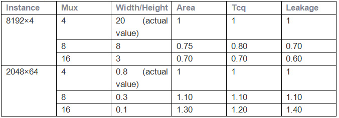
To quantify the impact of Mux on PPA, we select the Memory Compiler of IPSoar 22nm process node, and compare the Area, Clock-to-Output delay (Tcq) and Leakage power consumption of two typical instance specifications (8192×4 and 2048×64) when Mux is set to 4, 8 and 16. For the convenience of comparison, all indicators are normalized with Mux=4 as the benchmark (value=1):
Data Analysis
•Rule a — Correlation Between Shape and Area: Under different Mux values, SRAM has completely different shapes, and the area also changes accordingly. For instances with a large Word count (8192) and small Bit width (4), increasing Mux can significantly shorten the excessively long BL, make the array more compact, and the area drops from 1 to 0.7, which brings obvious benefits.
•Rule b — Correlation Between Speed and Timing: Also taking 8192×4 as an example, when Mux increases from 4 to 16, Tcq improves from 1 to 0.7, and the speed increases by about 30%. This is because the excessively long BL is greatly shortened, eliminating the main delay bottleneck. On the contrary, for instances with a small Word count and large Bit width (such as 2048×64), increasing Mux will further stretch the already very long WL, leading to simultaneous deterioration of speed and area.
•Core Conclusion: Different Mux values will present different shapes and PPA performances, making it the cornerstone parameter for selecting instances in MC.
2. Bank: Cutting the Memory Array to Obtain Higher Read and Write Performance at a Larger Area Overhead
Facing the increasingly diverse design demands under advanced processes, relying only on Mux adjustment often cannot fully meet the trade-off requirements between speed and area. At this time, Bank partitioning becomes another important parameter tuning method.
Physical Principle of Bank
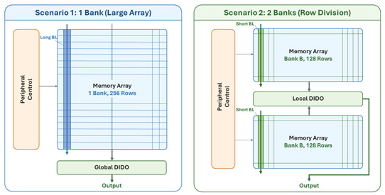
The essence of Bank is to divide the entire memory array into multiple independent sub-banks along the column direction. Each Bank has its own independent peripheral circuits, including Sense Amplifiers, Column Decoders and local control signals. Increasing the number of Banks means breaking a long bit line that runs through the entire array into multiple shorter sub-bit lines, thus significantly reducing the load capacitance on a single BL.
Specifically, different Bank selections lead to different partitioning methods of the array in the Column direction. For example, for an instance with a total Row count of 256: when Bank=1 is selected, all 256 rows belong to the same Bank; when Bank=2 is selected, the array is divided in half, and each Bank carries 128 rows; when Bank=4 is selected, each Bank only carries 64 rows. The more Banks there are, the fewer rows a single Bank has, the shorter the corresponding WL and BL, and the faster the read and write speed.
Trade-off Logic of "Trading Area for Speed"
•Performance Improvement Mechanism: After Bank partitioning, the length of each bit line is shortened proportionally, the parasitic capacitance decreases accordingly, the load that the sense amplifier needs to drive is greatly reduced, and the signal transmission delay is significantly reduced, thus effectively improving the read and write speed. This is a typical "trading space for time" strategy.
•Area Cost: Each Bank needs to be equipped with a complete set of peripheral circuits. The more Banks, the higher the proportion of duplicated peripheral circuits, and the larger the total chip area. At the same time, additional isolation and wiring space are required between Banks.
•Power Consumption Change: Due to the increase in area and the number of transistors, the static Leakage power consumption usually rises with the increase of the number of Banks. However, in high-frequency working scenarios, the reduction of dynamic power consumption brought by the decrease of bit line capacitance may partially offset or even exceed the increase of leakage, which needs to be evaluated in combination with the specific operating frequency.
•Applicable Scenarios: When the chip has strict requirements for read and write speed (such as high-performance computing, AI accelerators, etc.) and is relatively tolerant to area and power consumption, increasing the number of Banks is a very effective architecture solution.
Instance Data: Taking IPSoar 22nm MC as an Example
Based on IPSoar 22nm MC, we compare the normalized PPA data when Bank is set to 1, 2 and 4 for the instance with the specification of 1024×64:

Data Analysis
•When Bank increases from 1 to 4, the area increases by about 30% (1 → 1.3), while Tcq improves by about 25% (1 → 0.75), which brings a significant speed increase, confirming the expectation of "trading area for speed".
•At the same time, Leakage rises from 1 to 1.5, with an increase even exceeding that of the area, indicating that the leakage contribution of peripheral circuits cannot be ignored.
•Important Reminder: Due to the additional routing and circuit delay introduced by the increased area, some instances may experience overall timing deterioration when the number of Banks is too large due to the increased global load caused by the complication of logic circuits and the increase of area. Therefore, the selection of Banks is not "the more the better". In the end, it must be based on the actual data generated by MC, and make a comprehensive decision in combination with specific design objectives.
3. Vt: Regulating Peripheral Circuit Threshold Voltage to Flexibly Balance Speed and Leakage Power Consumption
Different from the first two parameters which start from the "array structure", the Vt (threshold voltage) option starts from the "transistor level". It modifies the threshold voltage of the transistors in the SRAM peripheral circuits, providing customers with more flexible choices between Speed and Power.
Physical Connotation of Vt
The threshold voltage (Vt) of a transistor is the core parameter that determines its switching characteristics, directly affecting two key indicators of the circuit:
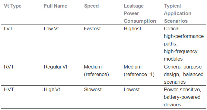
•Speed: The lower the Vt, the higher the on-state current of the transistor, the smaller the gate delay, and the faster the circuit switching speed.
•Leakage: The lower the Vt, the Subthreshold Leakage increases exponentially, and the static power consumption rises sharply.
Therefore, the selection of Vt is essentially a precise game between the "performance ceiling" and the "power consumption budget". Memory Compiler usually provides three typical Vt options for designers to choose according to application scenarios:
Instance Data: Taking IPSoar 22nm as an Example
Based on the IPSoar 22nm process, we compare the normalized Speed and Power data under three Vt options (RVT, HVT, LVT) for the instance with the specification of 4096×32:

Data Analysis
•No change in area: Vt only changes the doping and threshold of the transistor, and does not change the layout size, so the area remains consistent (all equal to 1) under the three Vt options.
•Seesaw between speed and power consumption: LVT reduces Tcq to 0.85 (speed increase by about 15%), but the leakage power consumption surges to 3 times; HVT reduces the leakage power consumption to 0.7 (saves 30%), but sacrifices about 15% of the speed. This is the core value of Vt adjustment — without changing the array structure, it provides additional degrees of freedom for design through device-level optimization.
•Application Suggestion: In actual SoC design, LVT can be selected for SRAMs on performance-critical paths, and HVT can be selected for SRAMs with sufficient timing margin and high power consumption sensitivity. Global PPA optimization can be achieved through hybrid configuration.
4. Summary: Collaborative Optimization Strategy for the Three Parameters
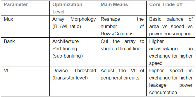
Mux, Bank and Vt provide rich parameter tuning dimensions for SRAM PPA optimization from three different levels: array morphology, architecture partitioning and device threshold. The three parameters can be configured independently or combined collaboratively to form a hierarchical optimization strategy:
Collaborative Optimization Suggestions
•Step 1 — Mux sets the basic tone: According to the Word/Bit ratio of the instance, select an appropriate Mux to determine the basic shape of the array and the BL/WL ratio, and complete the preliminary area optimization.
•Step 2 — Bank improves performance: If the speed still does not meet the requirements, increase the number of Banks to cut the array, and obtain significant timing improvement at a controllable area cost. It needs to be emphasized that for some memory instances, after the number of Banks increases, the speed does not necessarily increase due to the complication of logic circuits and the increase of global load caused by area growth.
•Step 3 — Vt fine-tunes performance: After the structure is determined, the final Speed/Power fine-tuning is carried out at the peripheral circuit level through the Vt option to achieve local optimization.
•Final Verification: All parameter combinations are subject to the actual PPA data output by MC, and comprehensive trade-off is carried out in combination with the specific constraints of the project (area budget, timing signoff, maximum power consumption).
Conclusion
A deep understanding of the physical meaning behind Memory Compiler parameters is the only way for every chip design engineer to grow from "being able to use the tool" to "being good at using the tool". We hope the disassembly in this article can help you handle memory IP selection more confidently, lock in the optimal PPA scheme as early as possible in the early stage of the project, and effectively avoid the risk of repeated back-end iterations. IPSoar will continue to output more high-quality hardcore technical content, and work with industry colleagues to promote the innovation and development of memory IP technology.
Exclusive Quick Optimization Suggestion for IPSoar Memory Compiler
To solve the SRAM selection problem, IPSoar has launched the MindExplore tool. Users only need to set the Word, Bit and operating frequency, and the tool can enumerate all compliant instances. It also supports sorting by area and power consumption indicators, helping customers bid farewell to tedious manual comparison and select the most suitable solution in one step.
This tool supports both GUI mode and batch command mode, making it more convenient for customers to select SRAM instances efficiently.

Zhou Bin, COO of IPSoar microelectronics, said: "Memory Compiler IP is the core basic module in SoC chips. IP vendors should not only deliver the IP Design Kit to customers, but also output supporting technical understanding and engineering experience. The domestic chip design industry is developing rapidly, and different teams have uneven process accumulation. We insist on doing serialized technical popularization, hoping to open up the design understanding and parameter tuning experience we have accumulated on Memory Compiler, help domestic design teams avoid pitfalls and improve project success rates. In the future, IPSoar microelectronics will continue to polish domestic Foundation IP products, continuously output high-quality technical content, grow together with the domestic chip ecology, and contribute to the high-quality development of the local chip industry."